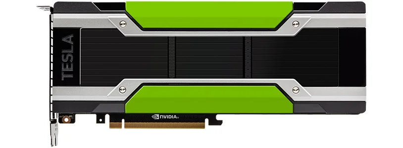
NVIDIA Tesla P100
3,584
CUDA Cores
16GB
VRAM
732
GB/s

Technical Specifications
3,584
CUDA Cores
1190
Base MHz
1328
Boost MHz
16GB HBM2
4096-bit bus
Performance
9.3
FP32 TFLOPS
18.7
FP16 TFLOPS
250W
TDP
Cloud Availability
0
Available Instances
$0.00/hr
Starting Price
Detailed Specifications
| Architecture | Pascal (Unknown) |
| Release Date | 2016-06-20 |
| Launch Price | $10,000.00 |
| Process | 16nm |
| Transistors | 15.3B |
AI Features
none
Tensor Cores
Disabled
Transformer Engine
Not Supported
Flash Attention
Physical Specifications
Dimensions
10.5in
Length
4.4in
Width
2-slot
Height
Top GPUs for Training and Inference
| Category | Rank 1 | Rank 2 | Rank 3 |
|---|---|---|---|
| Best for Training | NVIDIA H200 | NVIDIA H100 | NVIDIA B200 |
| Best for Inference | NVIDIA A40 | NVIDIA A100 | NVIDIA A10 |
Compare GPU specifications and cloud instances to find the best GPU for your workload.