NVIDIA H100
14,592
CUDA Cores
80GB
VRAM
3000
GB/s
Technical Specifications
14,592
CUDA Cores
1410
Base MHz
1830
Boost MHz
80GB HBM3
5120-bit bus
Performance
67
FP32 TFLOPS
2000
FP16 TFLOPS
700W
TDP
Cloud Availability
11
Available Instances
$1.47/hr
Starting Price
Detailed Specifications
| Architecture | Hopper (Unknown) |
| Release Date | 2022-03-22 |
| Launch Price | $30,000.00 |
| Process | 4nm |
| Transistors | 80B |
AI Features
Gen 4
Tensor Cores
Enabled
Transformer Engine
Supported
Flash Attention
Physical Specifications
Dimensions
10.5in
Length
4.4in
Width
2-slot
Height
About H100 GPU
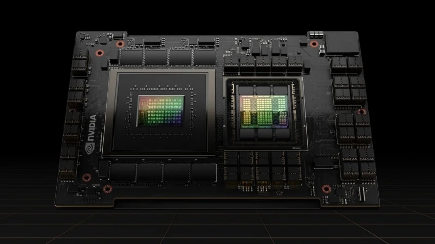
The NVIDIA H100 is a powerful GPU designed for AI/ML workloads, offering exceptional performance for both training and inference tasks. With 80GB of VRAM and 14,592 CUDA cores, it provides the memory capacity and computational power needed for modern deep learning models.
Released in 2022, the H100 features Hopper architecture with advanced AI accelerators including Tensor Cores and Transformer Engine support. This makes it ideal for large language models, computer vision tasks, and generative AI applications.
When considering cloud rental options for the H100, pricing starts at $1.47/hour from various providers. This GPU offers excellent price-to-performance for AI training workloads, with its high memory bandwidth of 3000 GB/s enabling fast data transfer for large datasets.
The H100 features CUDA compute capability 9.0 and is compatible with all major deep learning frameworks including PyTorch, TensorFlow, and JAX. Its 4nm manufacturing process ensures efficient power consumption relative to performance output.
Rent H100 from Our Partners
Get started quickly with these trusted GPU cloud providers. We may earn a commission when you sign up.
External Resources
Learn more about GPUs from these authoritative sources:
Official CUDA programming guide
NVIDIA GPU Specifications →Official NVIDIA GPU specs
TechPowerUp GPU Database →Comprehensive GPU specifications
CUDA Compute Capability Guide →GPU compute capability reference
What You Need to Know About the H100
Complete Specifications for the NVIDIA H100
Get detailed technical specifications for the NVIDIA H100 including VRAM capacity of , CUDA core count, Tensor Core count, memory bandwidth, and CUDA compute capability of . This GPU is designed for demanding AI training, inference, and high-performance computing workloads. Understanding these specifications helps you determine whether it is the right fit for PyTorch, TensorFlow, or custom CUDA-based applications.
Compare NVIDIA H100 Cloud Rental Prices per Hour
Find the best cloud rental prices for the NVIDIA H100 across providers like RunPod, Vast.ai, Lambda Labs, and CoreWeave. GPUvec aggregates real-time pricing data so you can compare costs per hour, find available instances, and choose the most cost-effective provider. GPU cloud pricing for this model varies by region and instance type, so comparing multiple options can save significantly on compute costs.
Is the NVIDIA H100 the Right GPU for Your AI Workload?
Learn whether the NVIDIA H100 is the right choice for your specific AI and ML workloads. We cover use cases including large language model training, fine-tuning, inference serving, computer vision, scientific computing, and rendering. Compare its specifications and pricing against other GPUs like the H100, A100, and RTX 5090 to make an informed decision for your infrastructure needs.
Top GPUs for Training and Inference
| Category | Rank 1 | Rank 2 | Rank 3 |
|---|---|---|---|
| Best for Training | NVIDIA H200 | NVIDIA H100 | NVIDIA B200 |
| Best for Inference | NVIDIA A40 | NVIDIA A100 | NVIDIA A10 |
Compare GPU specifications and cloud instances to find the best GPU for your workload.