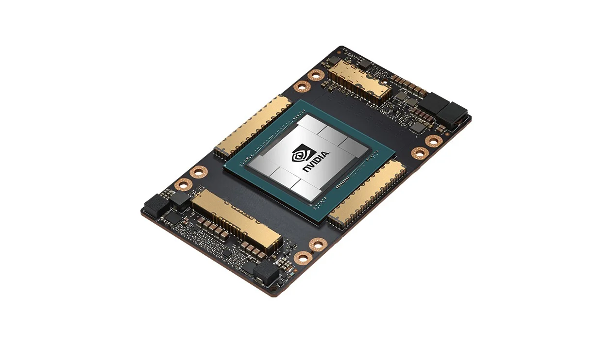
NVIDIA A100
6,912
CUDA Cores
40GB
VRAM
1555
GB/s
Technical Specifications
6,912
CUDA Cores
1410
Base MHz
1410
Boost MHz
40GB HBM2e
5120-bit bus
Performance
19.5
FP32 TFLOPS
312
FP16 TFLOPS
250W
TDP
Cloud Availability
11
Available Instances
$0.66/hr
Starting Price
Detailed Specifications
| Architecture | Ampere (Unknown) |
| Release Date | 2020-05-14 |
| Launch Price | $10,000.00 |
| Process | 7nm |
| Transistors | 54.2B |
AI Features
Gen 3
Tensor Cores
Disabled
Transformer Engine
Not Supported
Flash Attention
Physical Specifications
Dimensions
10.5in
Length
4.4in
Width
2-slot
Height
About A100 GPU
The NVIDIA A100 is a powerful GPU designed for AI/ML workloads, offering exceptional performance for both training and inference tasks. With 40GB of VRAM and 6,912 CUDA cores, it provides the memory capacity and computational power needed for modern deep learning models.
Released in 2020, the A100 features Ampere architecture with advanced AI accelerators including Tensor Cores and Transformer Engine support. This makes it ideal for large language models, computer vision tasks, and generative AI applications.
When considering cloud rental options for the A100, pricing starts at $0.66/hour from various providers. This GPU offers excellent price-to-performance for AI training workloads, with its high memory bandwidth of 1555 GB/s enabling fast data transfer for large datasets.
The A100 features CUDA compute capability 8.0 and is compatible with all major deep learning frameworks including PyTorch, TensorFlow, and JAX. Its 7nm manufacturing process ensures efficient power consumption relative to performance output.
Rent A100 from Our Partners
Get started quickly with these trusted GPU cloud providers. We may earn a commission when you sign up.
External Resources
Learn more about GPUs from these authoritative sources:
Official CUDA programming guide
NVIDIA GPU Specifications →Official NVIDIA GPU specs
TechPowerUp GPU Database →Comprehensive GPU specifications
CUDA Compute Capability Guide →GPU compute capability reference
Top GPUs for Training and Inference
| Category | Rank 1 | Rank 2 | Rank 3 |
|---|---|---|---|
| Best for Training | NVIDIA H200 | NVIDIA H100 | NVIDIA B200 |
| Best for Inference | NVIDIA A40 | NVIDIA A100 | NVIDIA A10 |
Compare GPU specifications and cloud instances to find the best GPU for your workload.